|
|
OEM mass production pcb/power bank pcb assembly pcba manufacturer
Collect
NO Turnkey electronic fr4 flex ci
PCB Specifications
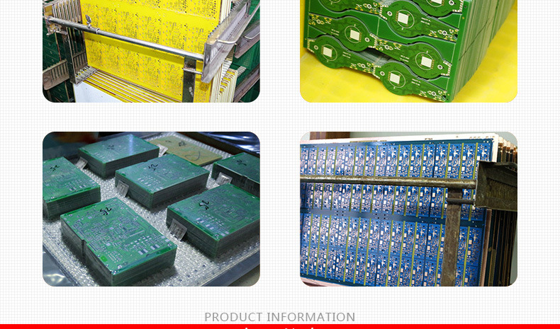
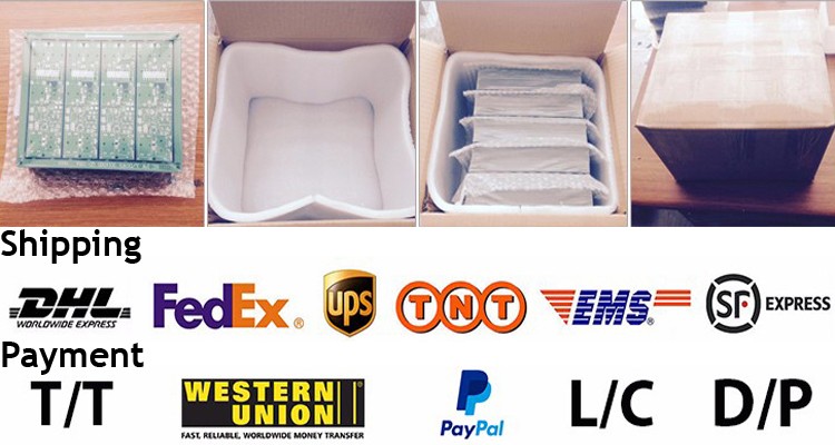
Supported Assembly Capabilities Different types of Assembly °THD (Thru-Hole Device) °SMT (Surface-Mount Technology) °SMT & THD combined °2-sided SMT and THD assembly Order Volume Allowed °1 to 5,000 boards Parts °Passives parts, smallest size 0201 °Fine pitch to 8 Mils °BGA, uBGA, QFN, POP and Zero-Lead chips °Connectors and terminals Component Package °Reels °Cut tape °Tube and tray °Loose parts and bulk PCB Board Measurements °Minimum measurement: 0.2″ x 0.2″ (5mm x 5mm) °Largest dimension: 15″ x 20″ (381mm x 508mm) Printed circuit board shapes °Oblong °Round °Slots and Cut outs °Complicated and Uncommon PCB board kinds °Rigid FR-4 boards °Rigid-Flex boards Assy procedures °Leaded process °Zero-Lead (RoHS) Design file formatting °Gerber RS-274X, 274D, Eagle as well as AutoCAD’s DXF, DWG °BOM (Bill of Materials) (.xls, .csv, . xlsx) °Centroid (Pick-N-Place Or XY file) Testing Processes °Visual Inspection °X-ray Inspection °AOI (Also known as: Automated Optical Inspection) °ICT (AKA: In-Circuit Test) °Functional testing Turnaround time periods °1 To 5 days for only printed circuit board assy °10 To16 days for full Turnkey Circuit Card Assy PCBA Testing We equipped a team of 3 skilled technical engineers who have many years experience in the field to put our strict testing flows and standards into practice. In the whole testing flow, by AOI, flying test and testing jig test we first test the flows of circuit board production including through-hole status, short circuit and appearance, etc. For some complicated craft flows e.g. in high precision or blind via boards, even only wafer analysis can discover testing problems.
Related
|
||||||||||||||||||||||||||||||||||||||||||||||||||||||||||||||||||||||||||||||||||||||||||||||||||||||||||||||||||||||||||||||||||||||||||||||||||||||||||||||||||||